
Physics - Mr. Sreekumaran Nair
1. Conductor - no energy gap Semi Conductor - It is of the order of 1 ev. Insulator - 6 ev (or) more than 6 ev.
2. When a semi conductor is heated more & more electrons get enough energy to jump across the forbidden energy gap from valence band to the conduction band, where they are free to conduct electricity. Thereby increasing the conductivity of a semi conductor.
3. In an intrinsic semi conductor the number of free electrons and holes is same.
4.
5.
6.
6. About 0.3V germanium .About 0.67V for silicon.
7. Transistor is a current controlled devices.
8. Reverse biased.
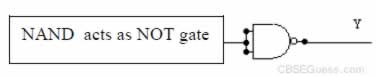
9.NAND GATE.
10.If ne/nh =1 . Hence A is intrinsic semi conductor.
If ne/nh <1 , ne<nh hence B is P-type.
11. For half wave rectification 50 Hz., For Full wave rectification 100Hz.
12. Mobility of an electron is defined as the drift velocity of electron per unit electric field, i.e. μe= Ve /E Mobility of a hole is defined as the drift velocity of hole per unit electric field, i.e. μh= Vh /E The electrical conductivity(σ) is the reciprocal of resistivity (p), therefore Conductivity, σ =1/ ρ = e(ne μe + nh μh ) Where ne & nh are free electron density & hole density respectively.
13. Diagram
14. The drift velocity of a charge carrier is proportional to electric E. Therefore V = eET/m ie. V a E But V cannot be increased indefinitely by increasing E . At high speed relaxation time (T) begins to decrease due to increase in collision frequency. S: so drift velocity saturates at thermal velocity (lOms-1). An electric field of 106 V/m causes saturation of drift velocity. Hence semi- conduction obey ohm’s law for low electrical field and above this field ( E < 106 V/m ) current becomes independent of potential.
15. The factors upon which transconductance of a transistor depend are as follows--
i) Geometry of the transistor
ii) Doping levels.
iii) Biasing of the transistors.
16. For faster action NPN Transistor is used .In an NPN transistor, current conduction is mainly by free electron ,whereas in PNP type transistor .it is mainly holes Since electron are more mobile than holes we prefer NPN for faster action as well as high conduction current.
17. graphs:
18. Because the energy gap for Ge ( Eg = 0.7 ev) is smaller than the energy gap for Si (Eg = 1.1ev ) . Moreover, the germanium diode is much more open to the danger of high temperature affect than silicon at high voltage.
19. The output of the AND gate is Y = A.B consequently the input of the OR gate are A and A.B . Then the final Y = A + A.B
20. The output of OR gate is A+B. Consequently, the inputs of AND gate are A+B & C Hence the Boolean equation for the given circuit is Y=(A+B).C
21) AND Gate using NAND GATE:-
22. NOT gate using NAND gate:-
Truth Table:-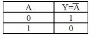
23. Here β =50
Ie =6.6mA
β =Ic/ Ib
24. Here
Ib = 100μA = 0.1mA
Ic = 3mA
a)β=Ic / Ib = 30
β = α / (1- α)
∴
α = 0.97
α = Ic / Ie
∴Ie = 3.1 mA
b) Δ Ib = 20μA 0.02 mA
βa.c. = Δ Ic / Δ Ib
βa.c. = 25
25. Here
Ic=95% of Ie = (95 / 100 ) Ie
Ie = (100 / 95) × 5 mA = 5.26mA
Ie= Ic+ Ib
Ib = 0.25 mA
26. Here
Ie = 5mA
Ic = 4.75 mA
Ie = Ic + Ib
Ib = 75 × 10-5 A
V = Ib Rb
V = 5V
Rb = V / Ib
Rb = 6.67 kΩ 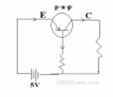
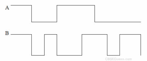
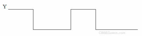
27. This is AND logic gate
Output wave form
28. Here
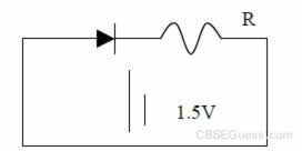
e.m.f of the source, E = 1.5V
Voltage drop across the diode , Vd = 0.5V
Maximum power rating of the diode
I = (P / Vd)
I= 0.2A
Potential drop across resistance R
V= E – Vd
= 1V
R = V / I = 1 / 0.2 = 5Ω
29. α = 0.96 , Ie = 7.2mA
α = Ic / Ie
∴Ic = α Ie = 6.91 mA
Ib = Ie –Ic
Ib = 0.29 mA.
30. β = 70
Ie = 8.8mA
Ie= Ic +Ib
∴Ib = 8.8 / 71
Ib = 0.124 mA
31. 31. Ib = 105 × 10-6 A Ic = 2.05 × 10⁻³A
β = Ic / Ib = 19.5
Also,
Ie = Ib + Ic = 2.155 × 10⁻³ A
α = Ic / Ie = 0.95
ΔIb = 27μA = 27 × 10-6 A
β = ΔIc / ΔIb = 24.1
32. ΔIe = 7.89 × 10⁻³ A
Δ Ic = 7.8 × 10⁻³ A
Now αa.c. = Δ Ic / Δ Ie = 0.9886
We have, βac= αac / (1-αac) = 86.72
Also,
βac = Δ Ic / ΔIb
∴ΔIb = Δ Ic / βac
ΔIb = (7.8 × 10⁻³ ) / (86.72)
ΔIb = 89.94 × 10⁻⁶A
CBSE Physics (Chapter Wise With Hint / Solution) Class XII (By Mr. Sreekumaran Nair)